


In 2023,IC Material Innovation Alliance (hereinafter referred to as "ICMtia"), Semiconductor Support Industry Branch of China Semiconductor Industry Association continue to work together with IC Branch of China Semiconductor Industry Association, IC Equipment Innovation Alliance, IC component Innovation Alliance, IC Encapsulation Innovation Alliance and China IC Testing Innovation Alliance to "Base on the new development stage, With the theme of "Building Core Development Pattern", the 25th China IC Manufacturing Annual Conference and Supply Chain Innovation and Development Conference were jointly held in Guangzhou from April 17 to 19. During this period, the Materials Alliance and the China Half Association Support Industry Branch held the 2023 China Semiconductor Materials Innovation and Development Conference.
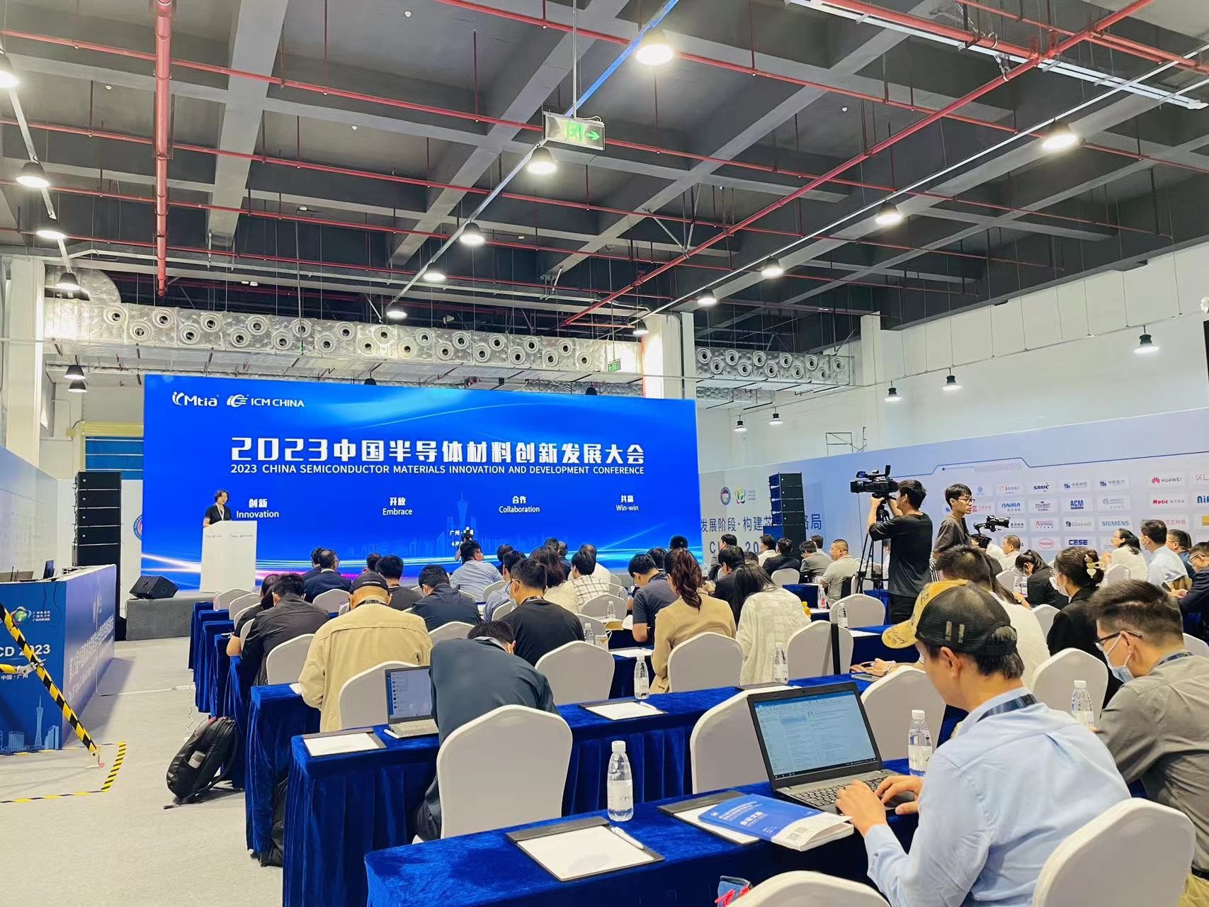
On the morning of April 19th, Ying Shi, secretary-general of ICMtia, hosted the summit forum of 2023 China Semiconductor Materials Innovation and Development Conference. More than 280 representatives from manufacturing and testing enterprises, Fabs and member enterprises attended the meeting.
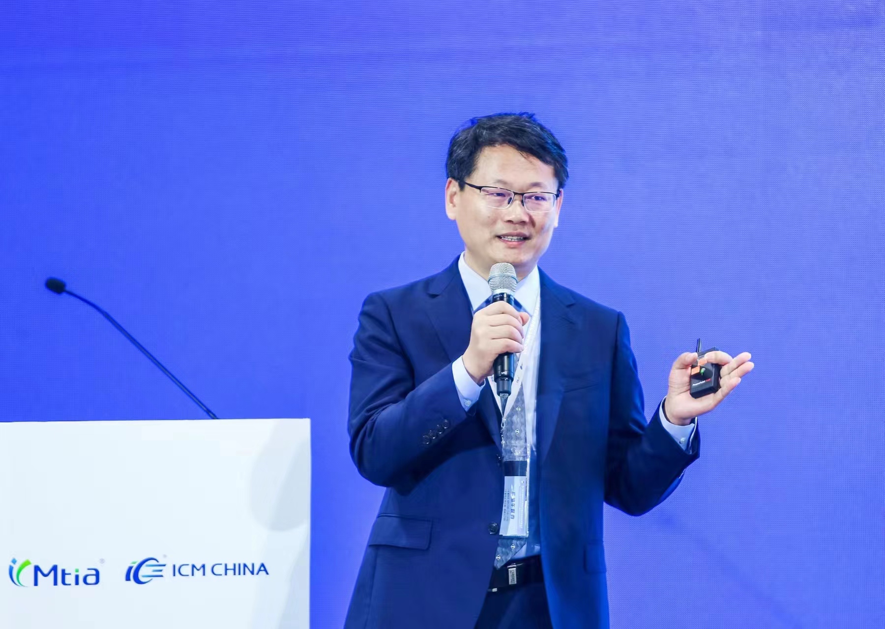
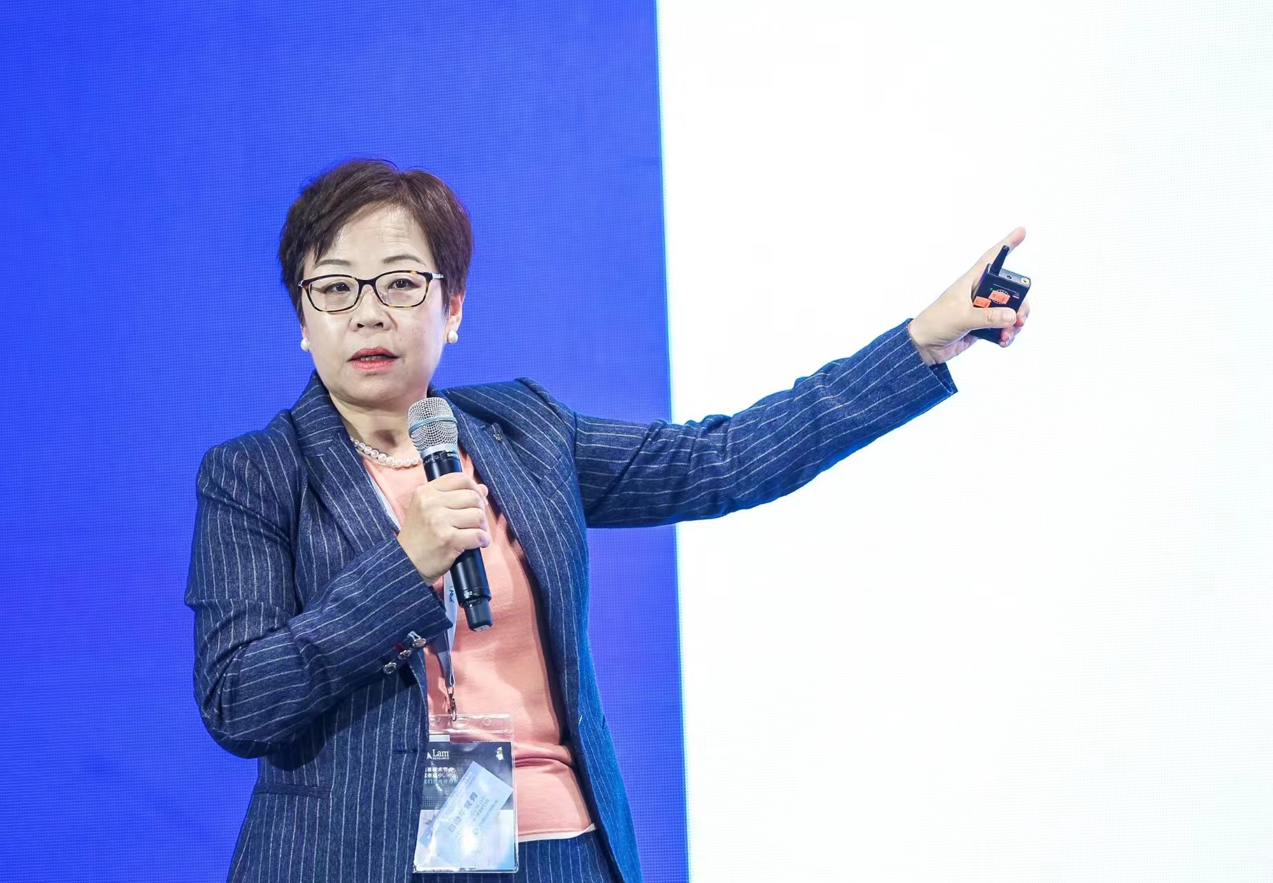
This conference specially invited the well-known experts in the industry, Dr. Ziqi Zheng, CTO of Tongfu Electronics Co., LTD.;Dr. Qingyu Wang, general manager of Shanghai Simgui Technology Co.,;LTD., Dr.Bing Li, general manager of Kempur Microelectronics Inc.; Hongxiu Peng, Deputy general manager of Anji Microelectronics Technology (Shanghai) Co., LTD., ; Dr.Yun Zhang, founder of Shinhao Materials LLC; Dr, Ms. Li Feng, deputy general manager of Shanghai Institute of Integrated Circuit Materials,;Dr. Karey Holland, chief strategist and co-founder of TECHCET.LLC, and Ying Shi, general secretary of the ICMtia, gave wonderful reports respectively, from international to domestic, from advanced technology to innovation path, from the field of closed test to materials. From the market trend to industry breakthrough comprehensive discussion of material industry development.
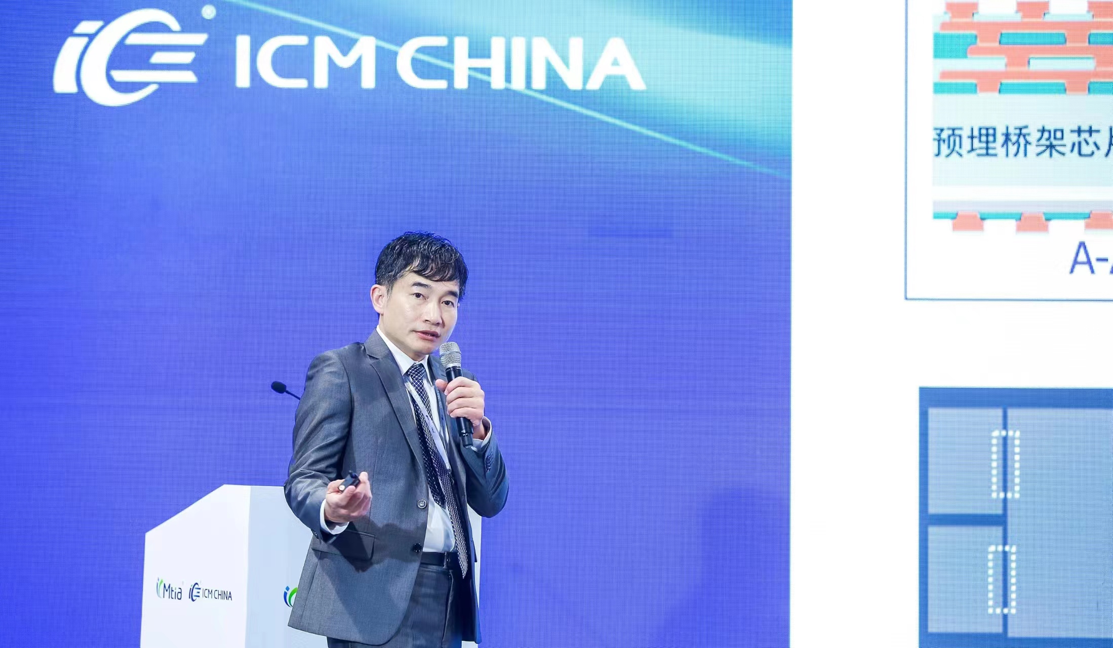
Dr. Ziqi Zheng, CTO of Tongfu Electronics Co., LTD., made a report titled "Trends of core integrated Packaging". In the report, he introduced the application range, technical characteristics and market advancement of core integrated packaging. He pointed out that currently core integrated design signals are homemade, which requires large-size packaging and high-density connection. Therefore, there are disadvantages such as high cost, high internal stress, very high I/O density and long cycle, and the technological breakthrough faces many challenges. Finally, the development status and future technology trend of domestic core integration are summarized.
Dr. Qingyu Wang, general manager of Shanghai Simgui Technology Co, LTD., pointed out in the report "Opportunities and Challenges brought by the Development of China's electric Vehicles to Domestic power semiconductors and materials" that the global automobile industry is developing towards the direction of electrification and intelligence. 80% of automobile innovation comes from the chip and electronics industry, among which the chip is the core component to support the electrification and intelligence of automobiles. The development of new energy vehicles in China brings good development opportunities to the domestic chip and power semiconductor industry.
In his report titled Development Trend of Photoresist and Local Diversified Supply Planning,Bing Li, general manager of Kempur Microelectronics Inc, introduced the evolution of photoresist technology in advanced manufacturing process of integrated circuits, and explained the technical requirements and material challenges of Iline, KrF, ArF, EUV and other types of photoresist. By analyzing the current situation and future development prospects of the chip manufacturing technology nodes in mainland China and corresponding to different types of photoresist market demand, combined with the different photoresist market and supply conditions and advanced IC process on the strict requirements of photoresist verification process, the development opportunities and challenges faced by China's photoresist were discussed. From the perspective of customers and suppliers, the paper discusses how to plan the local diversified supply of photoresist and raw materials, so as to achieve independent and safe supply.

Peng Hongxiu, Vice general manager of Anji Microelectronics Technology (Shanghai) Co., LTD., pointed out in the report "Integrated Circuit Wet Cleaning Technology" that with the size of advanced process node shrinking, wet cleaning has encountered more challenges, including small size defect control, HAR (high aspect ratio) structure cleaning and drying, compatibility of new materials, safety and environmental protection, and ultra-high purity quality requirements. Combined with the technical requirements of wet cleaning, the monolithic cleaning machine gradually replaced the trough batch processor to reduce defects, and the supercritical carbon dioxide was gradually introduced into use to avoid the collapse of the HAR structure. Peng Hongxiu, Vice general manager of Anji Microelectronics Technology (Shanghai) Co., LTD., pointed out in the report "Integrated Circuit Wet Cleaning Technology" that with the size of advanced process node shrinking, wet cleaning has encountered more challenges, including small size defect control, HAR (high aspect ratio) structure cleaning and drying, compatibility of new materials, safety and environmental protection, and ultra-high purity quality requirements. Combined with the technical requirements of wet cleaning, the monolithic cleaning machine gradually replaced the trough batch processor to reduce defects, and the supercritical carbon dioxide was gradually introduced into use to avoid the collapse of the HAR structure. From the perspective of safety and environmental protection, performance improvement and the combination of equipment/material advantages, the etching cleaning solution gradually transitioned from solvent base to semi-water-based and water-based. From the perspective of safety and environmental protection, performance improvement and the combination of equipment/material advantages, the etching cleaning solution gradually transitioned from solvent base to semi-water-based and water-based.
Dr. Yun Zhang, general manager of Shinhao Materials LLC, made a report titled "This copper is not that copper - the underlying design and implementation of grain structure", pointing out that advanced packaging is experiencing rapid growth which also brings many opportunities for innovation. Heterogeneous integration has special requirements that present new challenges for materials and processes. Using three different copper processes, she discussed copper-copper bonding requirements, which process is more suitable for copper-copper bonding requirements, and how the customer can achieve cryogenic bonding to ensure that other requirements are met.
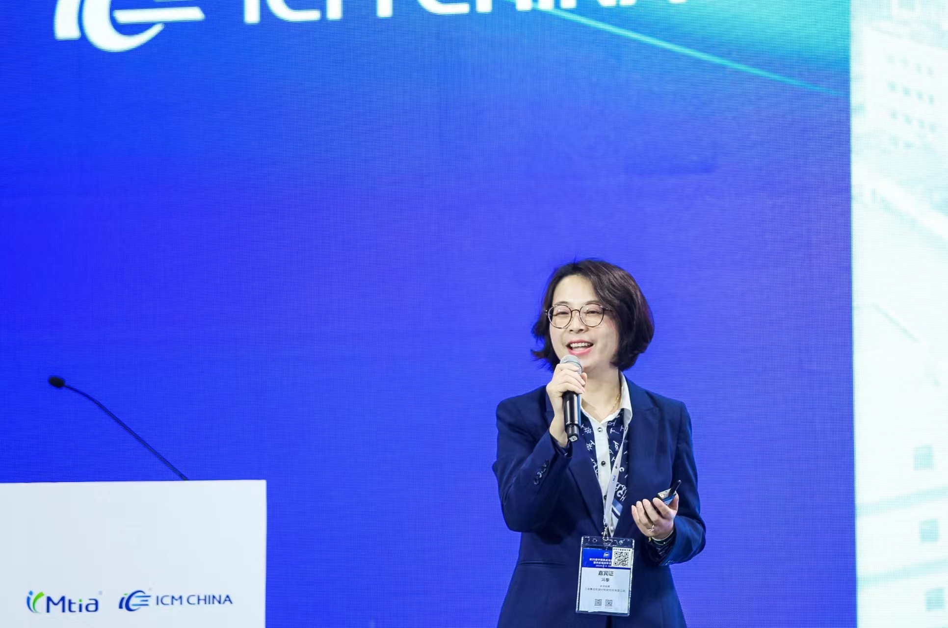
Ms Li Feng, deputy general manager of Shanghai Institute of Integrated Circuit Materials, delivered a report titled "Exploration of the Path of Technology Innovation of China's integrated circuit Materials". She introduced that with the deepening development of the integrated circuit industry, the development of the material industry and the upgrading of the path of technology innovation are becoming increasingly important. It is pointed out that new devices and new processes promote the innovation and development of new materials and new equipment, and new materials help semiconductor devices to develop into advanced manufacturing processes. The report also analyzes the current status and problems of IC material technology innovation in China, and puts forward new thinking directions for future technology innovation paths.
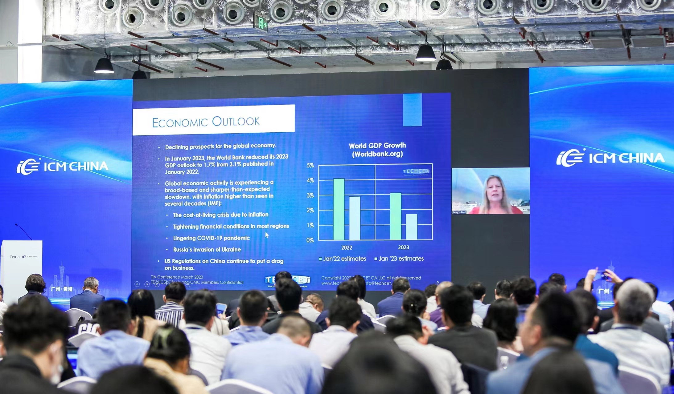
Dr. Karey Holland, chief strategist and co-founder of TECHCET.LLC, points out that the global materials segment is changing amid the trend of global chip investment expansion. In her report, "U.S. Wafer Expansion Trends and Materials Supply Chain Outlook," she highlights the increasing downward pressure on the international market due to changes in the international landscape. The opportunities and challenges that material suppliers who are seeking business expansion will face under the new trend are described.
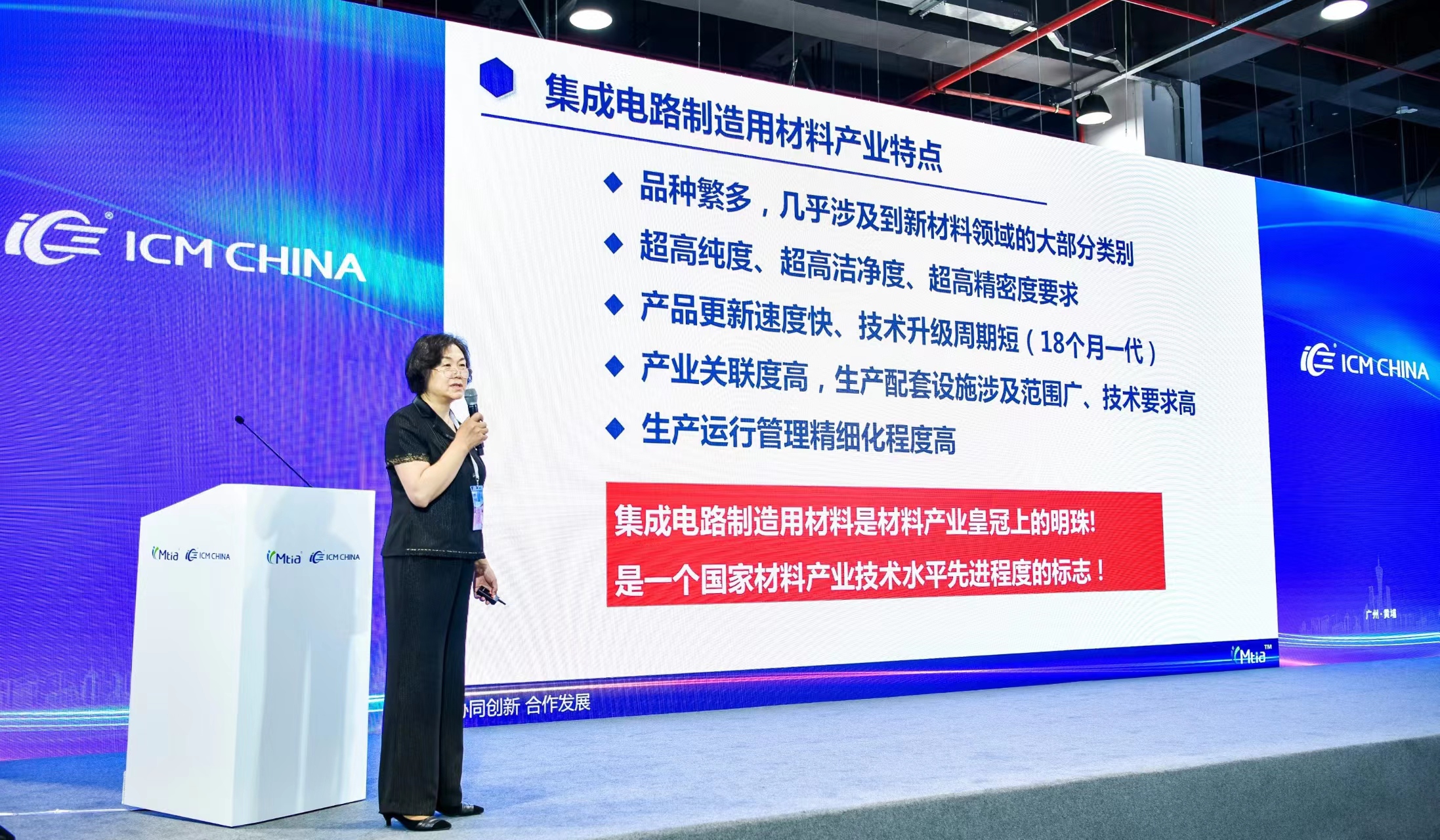
Ying Shi, secretary-general of the ICMtia, in the report Status Quo, Development Opportunities and Challenges of China's IC Manufacturing Materials Industry, analyzed the maturity of major products in domestic silicon materials, lithography materials, special electronic gases, process chemicals, CMP polishing materials, sputtering targets, packaging materials and other professional fields, and discussed the opportunities and challenges facing the development of the domestic industry under the new situation.
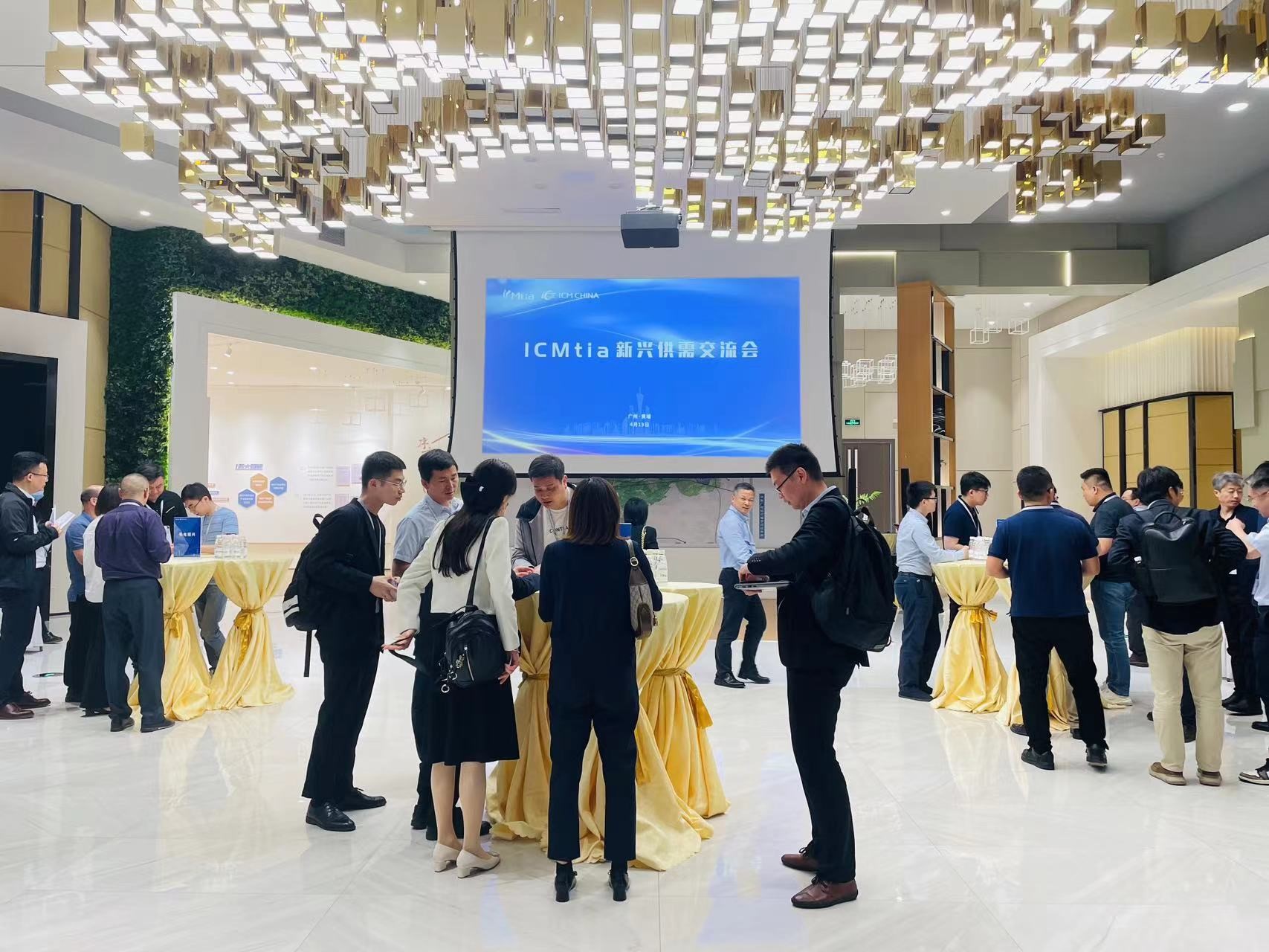
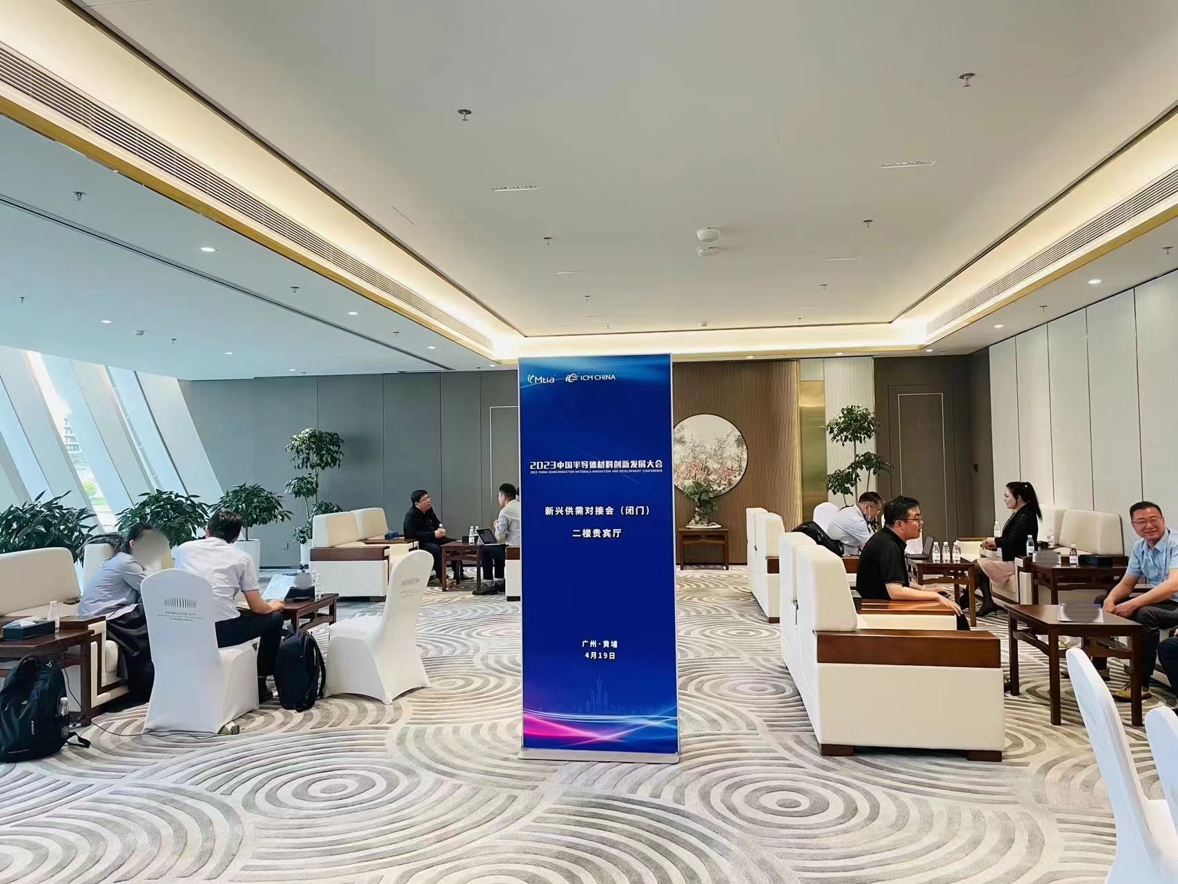
In the afternoon of the same day, ICMtia held the emerging supply and demand matchmaking meeting and exchange meeting in parallel. 5 domestic power device and advanced packaging enterprises and 40 domestic material suppliers had centralized or one-to-one closed-door communication, providing a platform and strong support for improving the domestic emerging semiconductor manufacturing local supply chain.