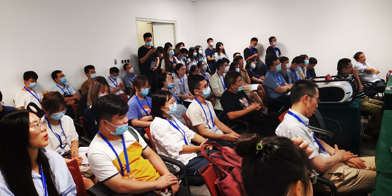


From July 8th to 11th, 2021, "China Materials Conference 2021" was held in Xiamen International Convention and Exhibition Center, Fujian Province. The conference has set up 51 branches and 3 sub-forums, covering the cutting-edge research fields of energy materials, environmental materials, semiconductor materials, superconducting materials, polymer materials, high-performance fibers and their composite materials, high-temperature alloys, superhard materials, biomedical materials, smart materials, etc. During the event, around 12,000 people attended the conference.
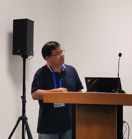
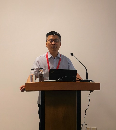
Organized by the Integrated Circuit Materials Industry Technology Innovation Alliance, and under the jointly support of the Shanghai Institute of Microsystems and Information Technology of the Chinese Academy of Sciences and the Beijing Multidimensional Electronic Materials Technology Development and Promotion Center, the "Advanced Microelectronics and Optoelectronic Materials Sub-Meeting" was held concurrently. Xi Wang, the Deputy Governor of the People's Government of Guangdong Province, served as the chairman of the "Advanced Microelectronics and Optoelectronic Materials Sub-Meeting". Academician Zhengping Wang of the Chinese University of Hong Kong was honorary chairman, and Academician Deren Yang of Zhejiang University, Chao Zhao, Institute of Microelectronics of Chinese Academy of Sciences, and Dr. Qinghuang Lin of ASML, jointly served as vice-chairmen. Mr. Chao Zhao, on behalf of Academician Xi Wang, gave an opening speech at the branch meeting. This "Advanced Microelectronics and Optoelectronic Materials Sub-meeting" has a total of 1 keynote speech, 13 invited reports, 17 oral reports, 19 posters, and more than 80 participants. The report covers the fields of microelectronics and optoelectronic materials, including: new storage materials such as MRAM, FRAM, PCRAM and RRAM; substrate materials such as Ge, Si, SOI, GOI and compound semiconductors; new display materials and other materials used in the manufacture of integrated circuits and optoelectronic devices; advanced packaging Materials; carbon-based functional materials such as carbon nanotubes and graphene; new two-dimensional materials such as CN3; material detection technology and methods; material design theory and calculation simulation, etc.
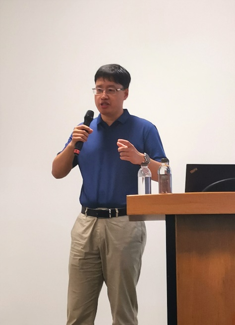
Professor Bin Yu from Zhejiang University gave a keynote speech titled "Application of Two-dimensional Materials in Post-Moore Electronics". Professor Yu introduced the development of integrated circuits along with Moore’s Law, believed that it has entered the post-Moore era, pointed out the limitations of silicon-based microelectronic materials, and proposed some potential applications of two-dimensional materials in post-Moore electronics. Quality integration and integrated design are becoming more and more important.
Researcher Zhitang Song from the Shanghai Institute of Microsystem and Information Technology, Chinese Academy of Sciences gave an invited report entitled "High-speed and low-power phase change storage materials and applications". Researcher Zhitang Song believes that with the rapid development of 5G, artificial intelligence, Internet of Things, and smart cars, the amount of data has exploded. Mass storage technologies and new architectures are needed to solve the current "storage wall" problem, and phase change memory is the most Potential next-generation mass storage technology. Researcher Zhitang Song introduced the team's systematic research work in recent years in the development of new phase change materials, high-speed reversible phase change mechanisms of phase change materials, new OTS gate materials, phase change memory process integration, and phase change memory product development.
Associate Professor Yi Yang from Tsinghua University gave you an invited report entitled "Non-Volatile Ferroelectric Memory Based on Hafnium-based Materials". Professor Yang believed that compared with traditional ferroelectric materials, hafnium-based ferroelectric materials are more compatible with CMOS technology; The advantages of high integration are more suitable for new types of ferroelectric memory. FeFETs based on hafnium-based ferroelectric materials have achieved process nodes as low as 10 nm, and can realize technologies such as Mbit-level storage and 3D stacking. FeFET based on hafnium-based ferroelectric materials has broad development prospects in the fields of new storage, storage-computing integration, and brain-like computing.
Professor Ping'an Hu from Harbin Institute of Technology gave an invited report entitled "Two-dimensional piezoelectric materials and flexible devices". Professor Ping'an Hu believed that two-dimensional piezoelectric materials have excellent photoelectric properties and piezoelectric coupling performance, compared to Traditional piezoelectric materials have the advantages of flexibility, compatibility with CMOS technology, easy processing and integration, etc., and are suitable for new self-driving photodetectors and flexible electronic skin devices. Based on the discovery of two-dimensional piezoelectric materials with the same polarization in the adjacent layer and the effective regulation of two-dimensional piezoelectric crystal domains, high-performance self-driving photodetectors and highly sensitive electronic skin devices have been realized. Two-dimensional piezoelectric material flexible devices have broad development prospects in the fields of low-power sensing, robotics and artificial intelligence.
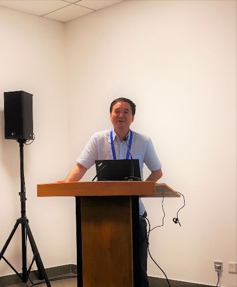
Professor Daquan Yu of Xiamen University introduced the development history of advanced packaging technology in the invited report on "New Material Challenges in Advanced Packaging". With the diversification of integrated circuit applications, emerging fields have put forward higher requirements for advanced packaging, and advanced packaging has become an increasingly important means to continue and expand Moore's Law. High-density TSV technology/Fan-Out fan-out technology has become the core technology of current advanced packaging due to its flexibility, high density, and suitability for system integration. Professor Yu believes that my country's integrated circuit packaging materials and technology are far from the international advanced level, and technological development is lagging behind. It is necessary to carry out collaborative innovation of industry, university, research and use, accelerate the pace of innovation, and reduce innovation costs. "Packaging companies + equipment companies + materials companies + scientific research institutions" collaborative innovation is of urgency, and it is necessary to organize collaborative research to meet the global technical challenges in the post-Moore era.
Professor Ran Liu from Fudan University gave an invited lecture entitled "Micro-nano pattern and device array preparation technology for organic functional materials based on selective growth". In view of the shortcomings of traditional inorganic methods and existing organic methods, Professor Liu’s team developed The research equipment for in-situ monitoring of vacuum and liquid phase was developed, highly original and recognizable surface and interface control research was carried out, and the micro-nano patterns and device arrays of organic functional materials were prepared by a novel selective growth method. Professor Liu Ran said that flexible electronic technology has unique flexibility and extensibility, can form smart packaging, wearable health care products, etc., and will become the core technology that promotes the popularization and large-scale application of the Internet of Things.
Professor Hongyu Yu from Southern University of Science and Technology presented the research progress of the research group in recent years in the field of wide-gap semiconductor devices in the invited report of "The Latest Research Progress of Wide-Gap Semiconductor Devices". The development of GaN process technology, the development of GaN product technology, the development of international SiC product technology and the development of my country's SiC product technology are introduced. Professor Yu believes that the international third-generation semiconductor industry represented by GaN and SiC has achieved a successful leap from R&D to large-scale mass production by the “four-wheel drive” of policies, capital, technology, and the market, and has entered rapid industrialization. development stage.
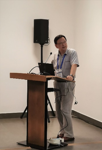
Professor Yuzheng Guo of Wuhan University, in an invited report on "Silicon Carbide Gate Oxide Interface", through calculations clarified that there is a significant low electron density layer SiOx at the interface, and found that the interface Si-Si structure is the main defect structure of the transition oxide layer, and it is also possible There are a small number of vacancy defects. In the thermal oxidation of SiC, the generation of interface carbon defects is inevitable. It is found through calculation that the carbon-carbon defects on the side of the interface SiC have an important impact on the performance of n-channel MOSFETs. Therefore, the specific structure types of carbon defects and their impact on the interface need to be focused attention. Professor Guo believes that in the interface passivation process, the introduction of N source and B source gas at the same time can further reduce the defect state.
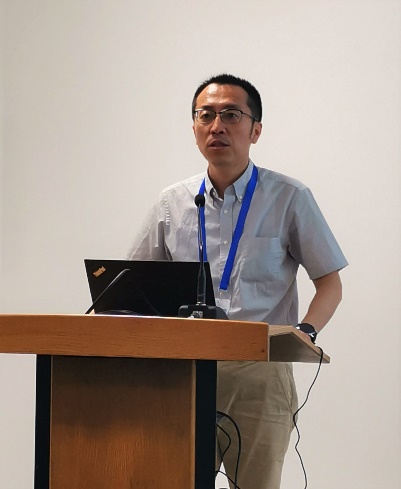
Associate researcher Yan Cai from the Shanghai Institute of Microsystems, Chinese Academy of Sciences gave an invited report entitled "Advanced Packaging Processes and Materials in Silicon-based Optoelectronics". Dr. Cai reviewed the current domestic and foreign developments in the field of silicon-based optoelectronics and optoelectronics. The latest progress of the silicon-optical integration research group of the Institute of Microsystems in the field of 2.5D/3D optoelectronic interconnection was introduced. The research group realized the TSV-based silicon-optical active board chip and the three-dimensional stacked high-speed germanium detector chip. Dr. Cai believes that 2.5D/3D hybrid integration of optoelectronics is a key technology to solve the power consumption, cost and performance of future silicon optical modules.
In addition, 17 teachers and students including Mengyu Chen from Xiamen University, Zhixia Shi from GRINM Resources and Environmental Technology Research Institute (Beijing) Co., Ltd., and Tiezhu Bo from China Building Materials Research Institute Co., Ltd. gave wonderful oral reports and shared their research results.
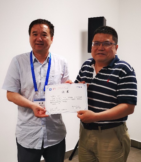
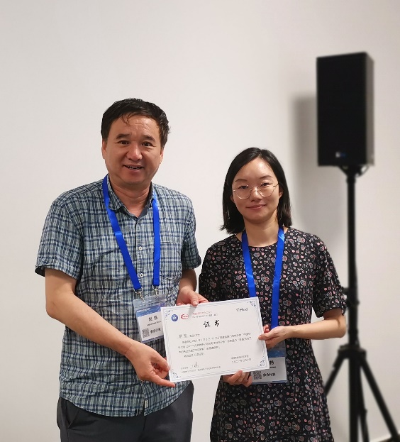
Yaru Huang from East China Normal University won the Best Poster Award of the club. The report of the conference was very exciting, the atmosphere of the conference was enthusiastic, and the audience was enthusiastic about questions. Participating representatives gained sufficient exchanges, which played a positive role in improving our country's academic level and technological innovation capabilities in the field of microelectronics and optoelectronic materials.